


GATE EC 2021 — Question 52

Semiconductor DevicesP-N junctionNAT2 marksMedium

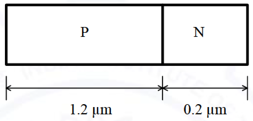
A silicon P-N junction is shown in the figure. The doping in the P region is \(5 \times 10^{16}\ \text{cm}^{-3}\) and doping in the N region is \(10 \times 10^{16}\ \text{cm}^{-3}\). The parameters given are Built-in voltage \((\Phi_{bi}) = 0.8\) V Electron charge \((q) = 1.6 \times 10^{-19}\) C Vacuum permittivity \((\varepsilon_0) = 8.85 \times 10^{-12}\) F/m Relative permittivity of silicon \((\varepsilon_{Si}) = 12\)
Question image
The magnitude of reverse bias voltage that would completely deplete one of the two regions (P or N) prior to the other (rounded off to one decimal place) is __________ V.
Practise the full 2021 paper
Challenge a friend: WhatsApp Telegram
From RENYXERAFree All-India Mock — every SundayA full GATE CS paper, exactly 180 minutes, ranked across India with your GATE score.
Practise more on P-N junctionTimed, in the real exam interface · free to start

A GATE question every morning

One real past-paper question every morning for your branch, answer hidden until you tap. Free on Telegram.

Join
Stuck? Ask in the student group